Zajednički odjel za elektroničke elemente / poluvodičke integrirane sklopove (ED15/SSC37) Hrvatske sekcije IEEE poziva Vas na predavanje:
Life After Drift-Diffusion – Breaking New Ground in Semiconductor Device Modeling and why that Matters,
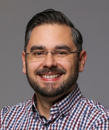
koje će održati Dr. Zlatan Stanojević, CTO, Global TCAD Solutions, Beč, Austrija. Predavanje će se održati u utorak 14. svibnja 2019. s početkom u 10:00 sati u Knjižnici ZEMRIS-a (D zgrada, 3. kat) na Fakultetu elektrotehnike i računarstva Sveučilišta u Zagrebu, Unska 3, Zagreb.
Predviđeno trajanje predavanja s raspravom je 60 minuta. Predavanje je otvoreno za sve zainteresirane, a posebno pozivamo studente. Više o predavaču i predavanju možete pročitati u opširnijem sadržaju obavijesti.
Short Bio
Dr. Zlatan Stanojevic received his Master and PhD degrees in electrical engineering from the Vienna University of Technology in 2009 and 2016, respectively. His current position is Chief Technology Officer (CTO) of Global TCAD Solutions (GTS) located in Vienna, Austria. The particular focus of Dr. Stanojevic's work has been on low-dimensional systems, i.e. FinFETs, nanowires, nanosheets and SOI. During his research career, Zlatan Stanojevic was responsible for the development of state-of-the-art computational tools for simulating low-field and high-field transport in low-dimensional systems, based on full band structure and the Boltzmann transport equation. He is the main author of the Vienna Schrödinger-Poisson quantum simulator and the GTS Nano Device Simulator (NDS).
Abstract
In the early 2000s, progress in semiconductor technology has shifted from being predominantly based on lithographic scaling to the development of so-called technology boosters, the most prominent being channel stress, high-k and metal gates, and the FinFET. The challenges faced in further scaling and the development of said technology boosters spurred a major push in research of advanced device modeling and simulation methods bordering on material science and promising to become the next generation of tools to aid technology development. Yet, the widespread adoption of advanced device modeling in simulation in commercial Technology Computer Aided Design (TCAD) software is lacking even today, more than 15 years later. The drift-diffusion model remains the workhorse of device simulation in TCAD with all the long and well-known problems and limitations. How could all that progress in semiconductor technology take place without profound paradigm shifts in the methodological backbone of commercial TCAD tools? Is TCAD in general and device simulation in particular actually relevant and what could future TCAD tools look like? Why aren’t we already using advanced methods such as NEGF to design transistors?
In this lecture we will discuss the experience gathered while developing the GTS Nano Device Simulator, the only commercially viable device simulator based on advanced charge transport modeling; we will show what it takes to achieve adoption of advanced device simulation by the industry and that sometimes the best method is not necessarily the most advanced one; and we will take a look at the challenges currently faced by the industry, for which TCAD when used in a smart way is anything but irrelevant.


