Hrvatska sekcija IEEE, Odjel za elektroničke elemente / poluvodičke integrirane sklopove pozivaju vas na predavanje
High Voltage Vertical Transistors Using Bulk Gallium Nitride,
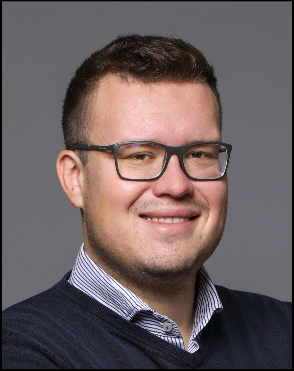
koje će održati Quentin Diduck, Ph.D., Eridan Communications, Inc., Santa Clara, CA 95050, USA
Predavanje će se održati u srijedu, 17. lipnja 2015. u 11 sati u dvorani TCR. Sadržaj predavanja i životopis predavača pročitajte u nastavku obavijesti.
ABSTRACT
Bulk gallium nitride (GaN) substrates with defect density on the order of 104 per cm2 are now commercially available. This material enables the fabrication of vertical GaN devices with large breakdown voltages, and enables excellent electrical performance. In this presentation, we discuss fabricating vertical transistors that have over a 1000V breakdown while supporting a positive threshold of 1V. The normally-off FET integrates a hetero-junction in the design to improve the transconductance and enable switching operation into the 10s of MHz.
A discussion of how horizontal and vertical channels can be used to support high frequency and high voltage operation will be covered. A range of breakdown voltage and on-resistance designs can be realized by adjusting the drift region doping and thickness. The nature of the design supports the fabrication of large drift regions that allow for multi-kV operation while supporting a non-destructive avalanche breakdown.
The high frequency performance and low on-resistance of this device design will enable a new class of power electronics that are very efficient and very compact. GaN bulk substrates are enabling the true capabilities of this material system.
SHORT BIOGRAPHY
Dr. Quentin Diduck joined Eridan Communications in 2014 as a Senior Member of Technical Staff. Dr. Diduck’s primary focus is on device physics and circuit integration on gallium nitride based semiconductors. Prior to joining Eridan Communications, Dr. Diduck worked for Avogy Inc. developing high-voltage vertical power transistors using free standing gallium nitride. Additionally he worked for Group4 Labs Inc. developing gallium nitride on diamond substrates and high power RF transistors using that material system.
Prior to joining Group4 Labs, Dr. Diduck was a post-doctoral researcher at Cornell University and worked for Professor Lester Eastman on developing GaN based - ballistic transport devices as well as high frequency RF components. During this time he developed novel fabrication methods for gallium nitride on diamond HEMT devices resulting in operating frequencies in excess of 90 GHz. With a firm belief in a holistic understanding of electrical engineering, he has devoted himself to a broad understanding of all electronic phenomena with experience from software engineering, mixed signal VLSI, to ballistic device simulation and fabrication. Currently Dr. Diduck holds four US patents and has three pending. Dr. Diduck completed his B.Sc. degree in electrical engineering at the University of Alberta, Alberta, Canada, in 1998, and then worked in industry for four years before completing his Ph.D. degree in electrical engineering at the University of Rochester, Rochester, NY in 2007.


